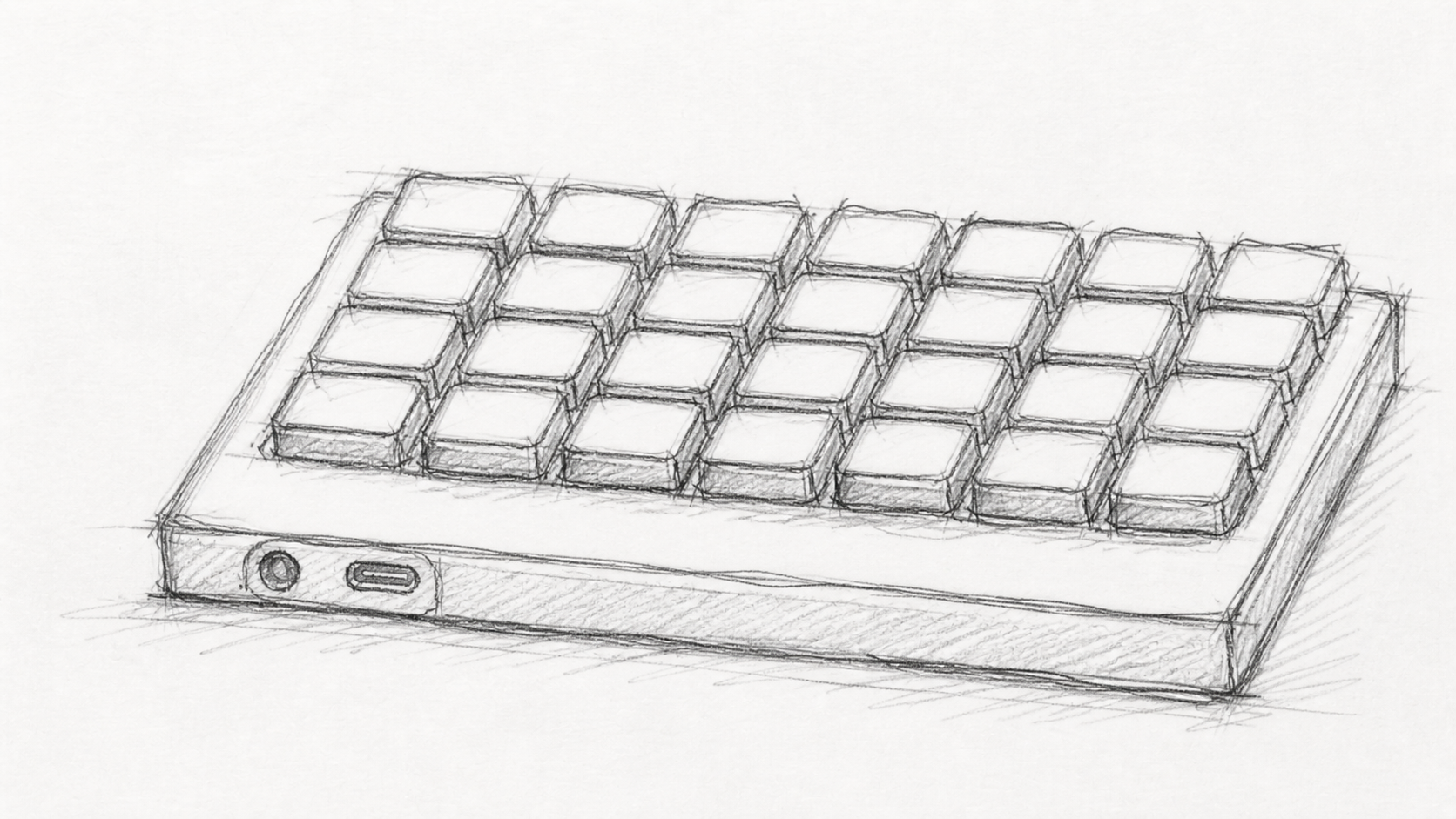
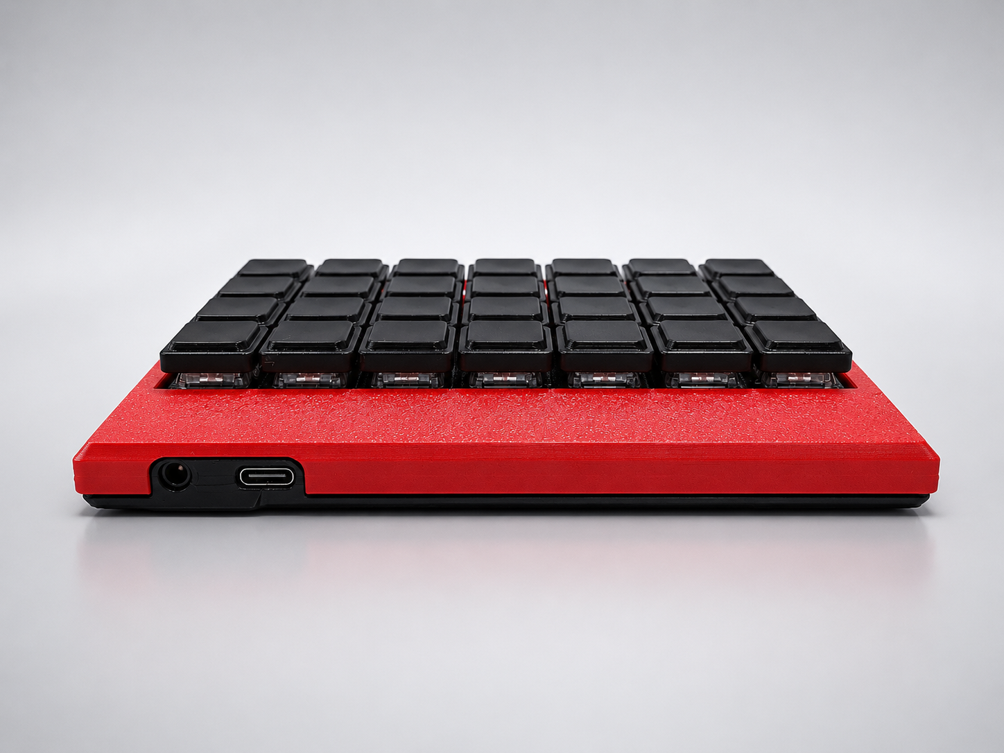
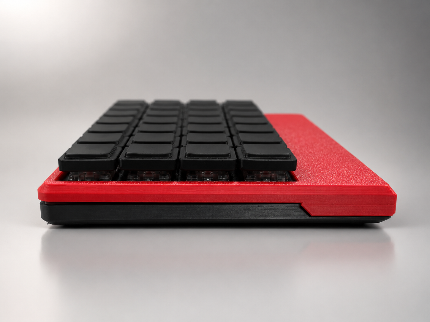
Thin Profile
The case was designed to stay as thin as possible while keeping enough strength for daily use.
Internal Wire Split Keyboard
A hand-wired keyboard build log for a thin split ergonomic keyboard using QMK firmware, Seeed XIAO RP2040, MCP23017 I/O expanders, and a 3D printed keyboard case.
This page is a work-in-progress project log.
Design notes, wiring details, QMK setup, and testing records are being added step by step .
Story
In November 2025, shortly after buying a 3D printer, I started building a split keyboard.
The first version was finished in about a month, but I was not satisfied with its appearance or feel. I decided to rebuild it without compromising the parts that bothered me.
Working around my job and other projects, and with a few pauses when the design stalled, it took about four months to finally complete this version.
The case was designed to stay as thin as possible while keeping enough strength for daily use.
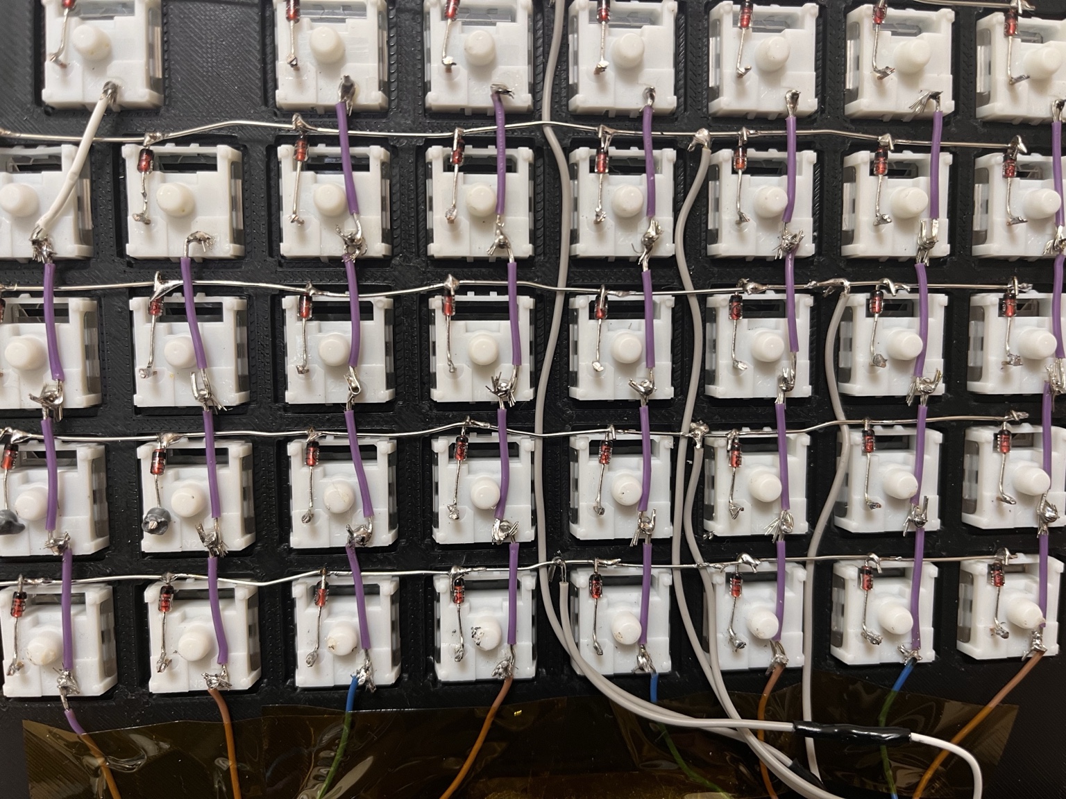
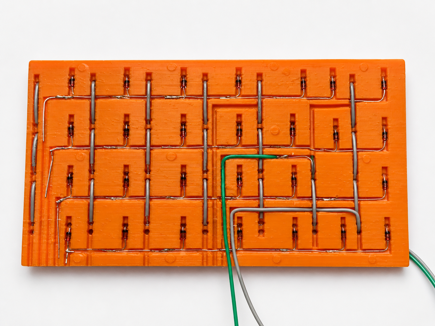
Wires are routed through grooves in the body so vibration is less likely to reach the internal wiring.
All joined parts use snap-fit structures, making the keyboard easier to take apart and assemble.
PCB sockets make it possible to reuse expensive switches, even if I rebuild it again.
I avoided designing a dedicated PCB and aimed to balance thinness, strength, and serviceability with hand wiring.
Production Note
This method is not intended for beginners or production-style builds. It has many wires, and soldering, continuity checks, and fitting everything inside the case take a lot of time.
In exchange, it focuses on long-term use by keeping the wiring contained and fixed inside the structure.
I wanted a hand-wired keyboard that could still be thin, clean, and practical as a daily split ergonomic keyboard.That led to an internal wiring keyboard structure that hides the matrix wiring inside the printed parts.
Concept
The wiring is hidden inside grooves in the plate instead of being exposed outside the keyboard. The goal is to reduce the unsupported wiring often seen in traditional hand-wired keyboard builds, making the keyboard thinner and less prone to wire breakage.
Comparison
The difference is whether the wiring is held in place by hand during assembly, or fixed inside the structure first.
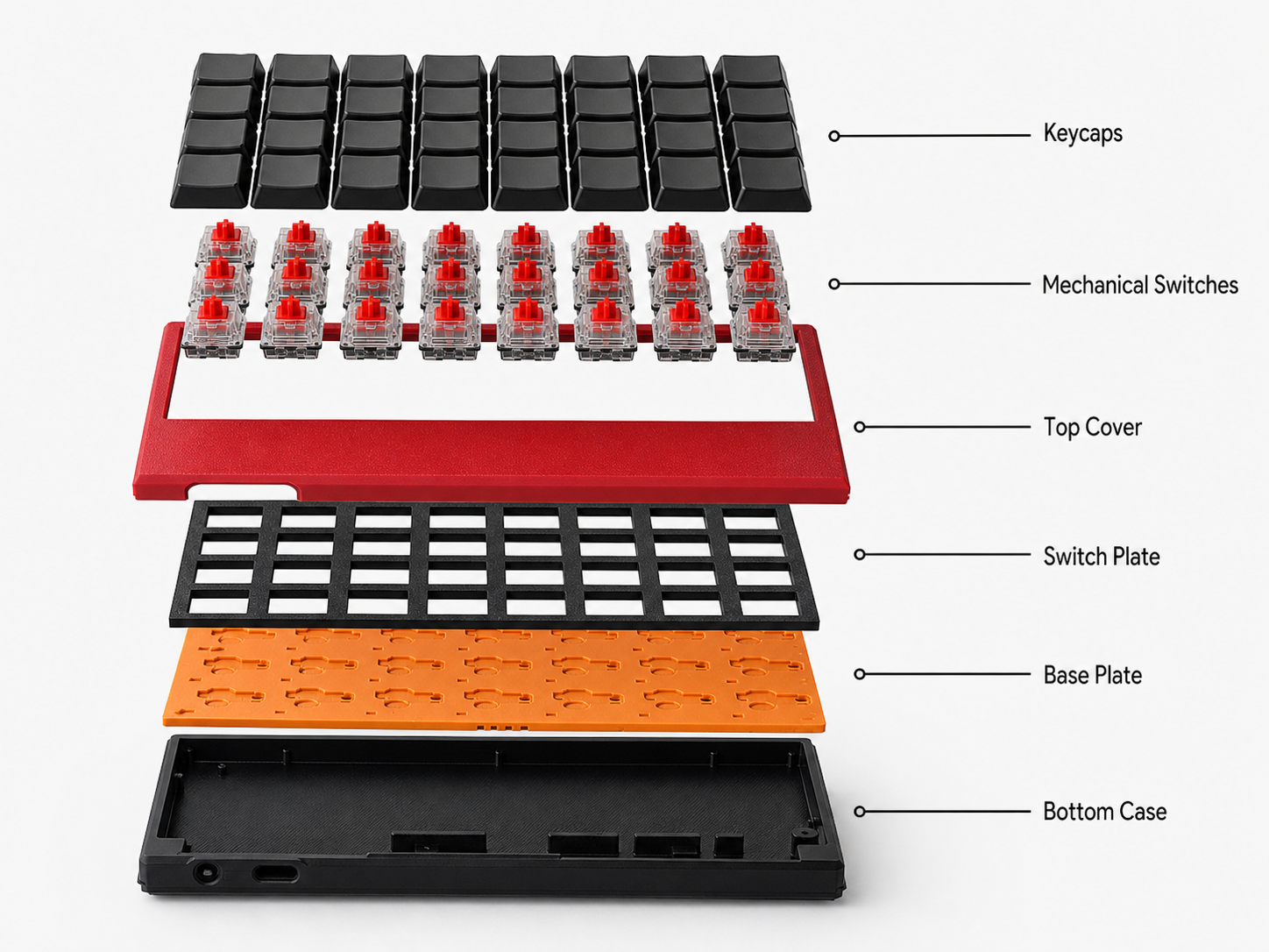
Structure
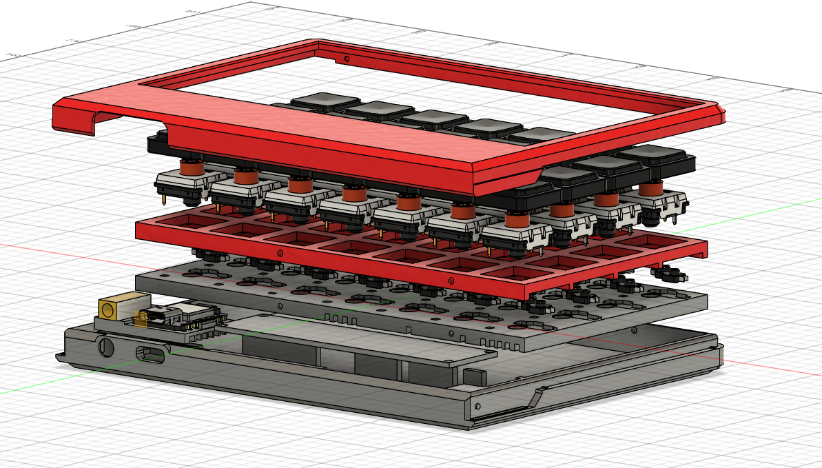
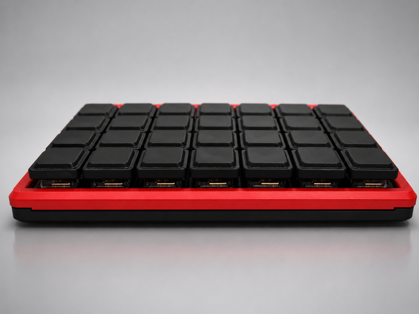
The keyboard reuses PCB hot-swap sockets without making a dedicated PCB. Combined with a 3D printed keyboard case and internal wiring routes, this makes a thinner profile possible while allowing key switches to be reused and replaced.
The key matrix uses internal wiring, avoiding the thickness and ordering process of a dedicated PCB.
Hot-swap sockets are reused so switches can be replaced.
Without stacking a PCB, the case and plate can stay thinner.
Process
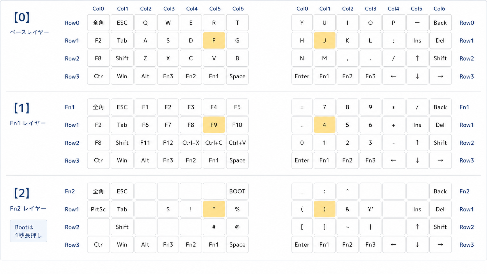
This mechanical keyboard build log covers the layout, internal wiring, 3D printed parts, QMK firmware, Seeed XIAO RP2040 keyboard controller, and MCP23017 I/O expander setup.
Decide the key count, split shape, size, thinness, and overall appearance. At this stage, the goal is not precise dimensions but deciding what kind of structure you want to make. This is the most enjoyable part of the process.
Note If the direction is vague here, later steps tend to create more rework.
Organize the key layout, row-column matrix, Seeed XIAO RP2040 keyboard controller, MCP23017 I/O expander, and left-right connection wiring.
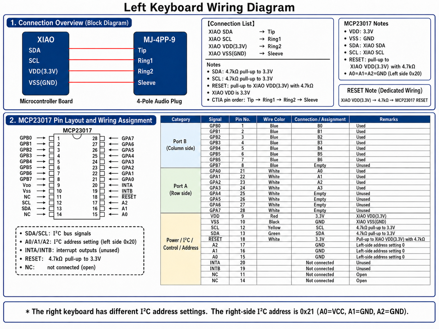
Note Wiring takes up more space than it first appears. Extra wires or inefficient routes can keep everything from fitting inside the case, so check the diagram repeatedly for missing paths and overlaps.
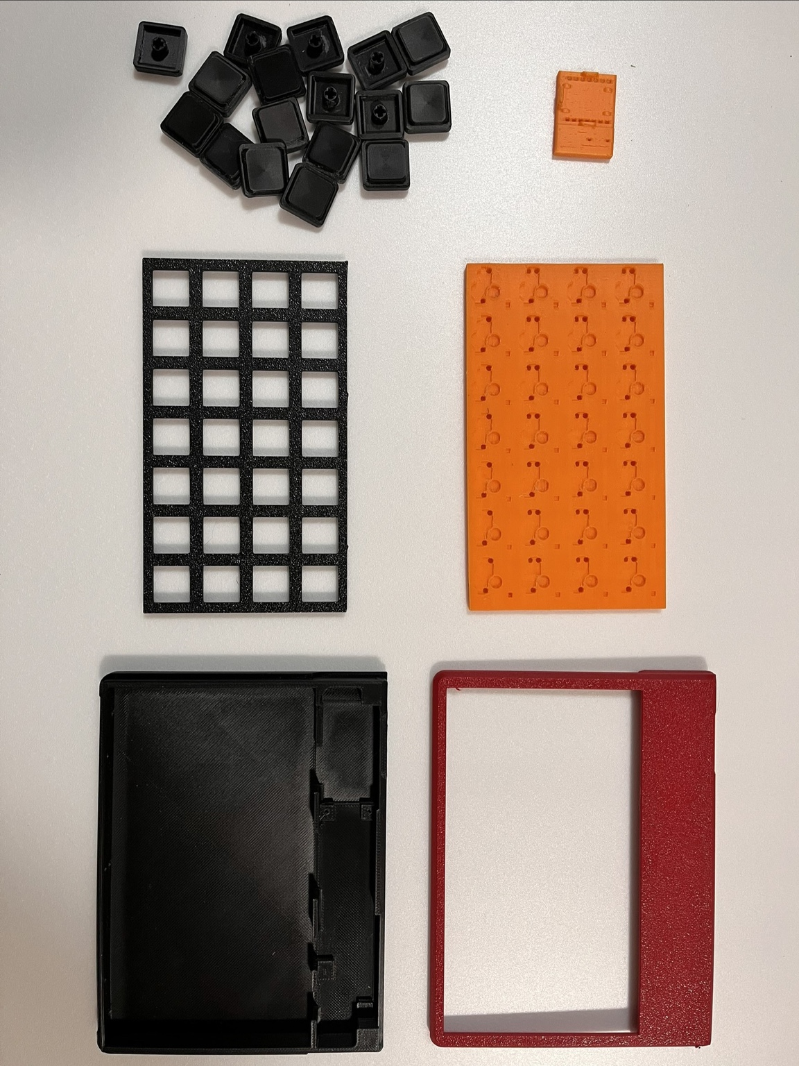
Design the top cover, switch plate, base plate, and bottom case as a 3D printed keyboard case. The wiring grooves, PCB socket positions, screw holes, and insert nut positions are also decided here. Because insert nuts can fail, the structure should allow multiple fixing points.
Note Because the wiring route is decided here, this design step changes the difficulty of the whole build.
Organize the required parts and tools: mechanical switches, PCB sockets, Seeed XIAO RP2040, MCP23017 I/O expanders, wire, screws, insert nuts, and soldering tools.
Note A purchasing mistake stops the work, so preparing the list matters.
Print the keyboard case parts and check dimensions, strength, and fit. Printing takes time, and failed prints or unsatisfying shapes make this one of the hardest steps.
Note Since this was my first time 3D printing, this was also the step where repeated revisions made me realize that buying something off the shelf might have been cheaper.
Fix the PCB sockets in their intended positions with two-part epoxy. I used a 30-minute curing type. After gluing the sockets, install the switch plate and key switches, place a weight on top, and leave it for a full day.
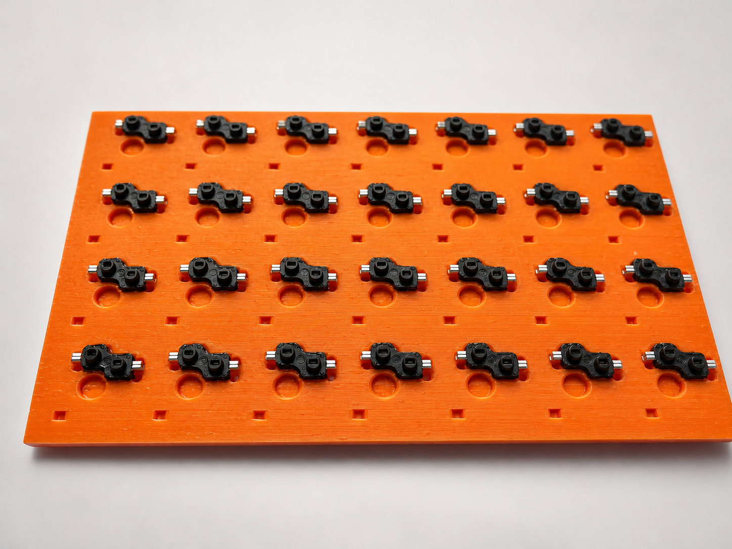
Note When inserting and removing switches, the surface around a socket can peel up. After the epoxy cures, adding a little more adhesive around the socket with a toothpick or other fine applicator helps make it more stable.
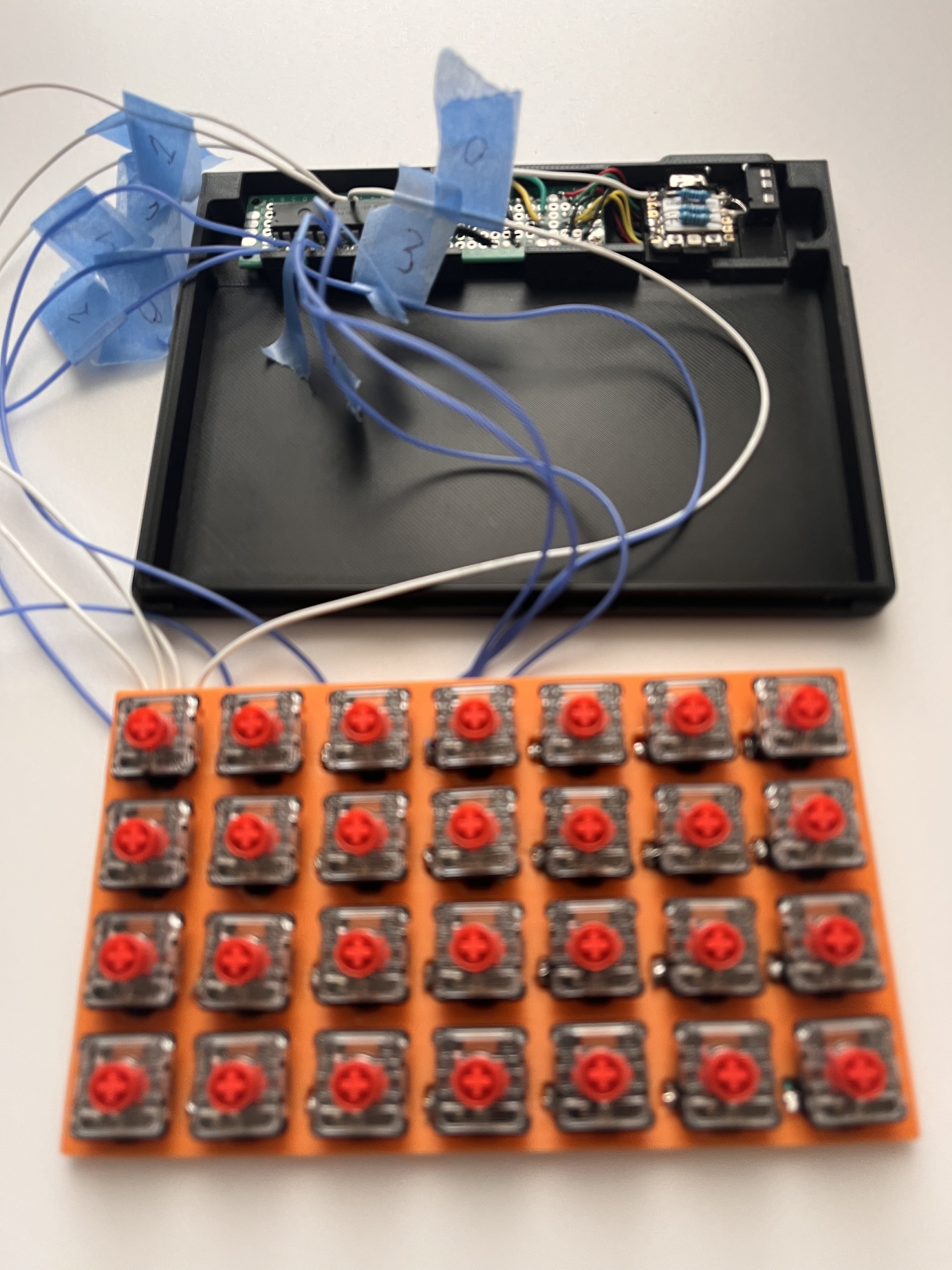
Run the wires through the grooves inside the plate, position them in place, and then solder them. By fixing the wiring routes on the structural side, this design aims to improve repeatability during assembly and reduce the risk of broken wires or shorts caused by vibration or contact.
Note When soldering on the base plate, press the wire into the groove with a small flat-head screwdriver so it does not leave a raised bump.
Connect the microcontroller and MCP23017 with temporary wiring, then check whether key input is recognized correctly. Compare the wiring, diode orientation, and QMK matrix settings one by one, and move to the next step only after confirming that there are no problems.
Configure the keymap, matrix, and MCP23017 I/O expander settings in QMK firmware. If the hardware layout and pin settings do not match, key input will not be recognized correctly.
This firmware is a QMK-based control program designed for the Take&Clock Works split keyboard. With an RP2040 at the center, it reads the left and right key matrices through I2C-connected MCP I/O expanders and operates as a 4-row by 14-column split keyboard. It also includes Fn layers, a symbol layer, and mirror layers for one-handed input.
Build the firmware in QMK MSYS, then copy the generated UF2 file to the XIAO RP2040.
Check every key input, the left-right connection, chatter, contact failure, and firmware settings. If something is wrong, correct the wiring, soldering, or QMK settings.
Follow / Download / Buy
Build records are being updated, and the 3D model data is available on GitHub.
Build progress and update information will be shared.
The 3D printable model data is available on GitHub. When printed, it can be used as case parts like the ones shown in the photo.
View 3D model on GitHub Printed models are planned for builders who do not have a 3D printer.